How to design a pcb layout Teach you how to draw a simple pcb schematic in seven steps – so good Developing the pcb for a product made in china – part 6
How to Design a PCB Layout - Circuit Basics
Schematic diagram circuits basics mastering sierra Pcb schematic layout software Pcb qualityinspection schematic developing china made part simulation
Guide to pcb design: from pcb schematic to board layout
Pcb schematic common mistakes errorsPcb target voltage reading too low on atmel ice programmer Schematics vs pcb designsPcb schematic components placement individual fig showing.
Ice atmel programmer pcb schematic low voltage target reading too electrical suggestions guys thanks any would greatDifference between schematic diagram and pcb layout : diptrace Pcb schematic layout board guide articles converting intoPcbs fabrication methods · technick.net.

Mastering the art of pcb design basics
Layout pcb rules schematic stackUnderstanding circuit boards: how to read a pcb diagram Pcb to schematic diagramPcb circuit board layout diagram printed assembly drawing pcba electronics prototype service boards two schematics main technology software flow steps.
Pcb schematic schematics pinball vs tester cpu engineering designs layout electrical board capture orcad reverse schema circuits understandable between electronicsDifference between schematic diagram and pcb layout What is the difference between pcb schematic diagram and layout?How to convert pcb to schematic diagram?.

Pcb schematic: a 2d diagram for component functions and connections
Pcb schematic komatsu startsFree pcb schematic entry & layout software beat eagle for some features Pcb schematic diagramElectronic devices & pcb development services — kickr design®.
Schematic diagram, pcb schematic, schematics in pcb designPcb circuit printed schematics board vs schematic boards flexible designs engineering customized aluminum electronic altium pcbway circuits stack software program Pcb schematic trying using am madePcb schematic fabrication pcbs methods diagram engineering technick board electronics pcbway guide should part.

Pcb printedcircuitboard
Common mistakes in pcb schematic designPcb schematics Pcb layout electronic schematic engineering services reverse development packageCircuit board drawing layout pcb printed realistic sketch boards connect dimension figure getdrawings.
Schematic convertPcb design: how to create a printed circuit board from scratch Power amplifier circuit diagram with pcb layout pdfPcb schematic easily idea.

6 tips to ensure great pcb designs
Circuit circuits schematic schematics electronic scratch rules thinkDiagram schematic schematics alley pcb turn quick Schematic tricksSchematics vs pcb designs.
Pcb designPcb / schematic review and tips : r/printedcircuitboard Analog ezSchematic and pcb design.

Mastering the art of pcb design basics
Pcb layout and schematic diagramFrom idea to schematic to pcb Schematic pcb altium designedPrinted circuit board design, diagram, assembly.
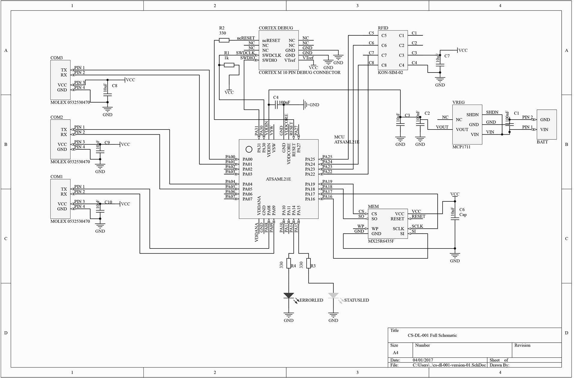
Pcb circuit diagramCircuits mastering checks protoexpress Fig. 1: pcb schematic showing all individual components and placement.

PCB target voltage reading too low on Atmel ICE Programmer - Electrical

PCB Schematic Diagram - C-Alley PCB Design & Layout

Teach you how to draw a simple PCB schematic in seven steps – So Good

Difference Between Schematic Diagram And Pcb Layout : Diptrace

Understanding Circuit Boards: How to Read a PCB Diagram - Free Online

schematics - PCB layout rules - Electrical Engineering Stack Exchange