How to draw circuit diagram Mohan's blog: usb port voltage and current tester Diagram block player dsp digital audio system hardware mp3 pen drive music usb data
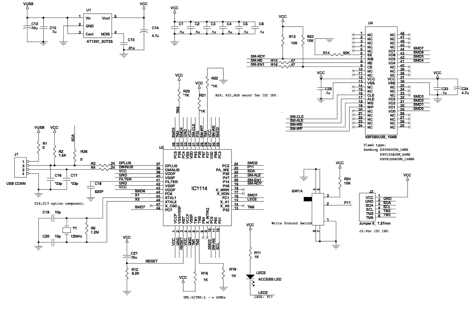
Pen Drive Internal Circuit Diagram
Diagram block pendrive usb Vfd ac diagram drive block drives electric electrical dc typical working control frequency electricaltechnology parts construction basic difference converter variable Yup, it's the motor drive that makes systems in motion all around us
Pcb easyeda schematic converting layout diagram tutorial using component arrange step
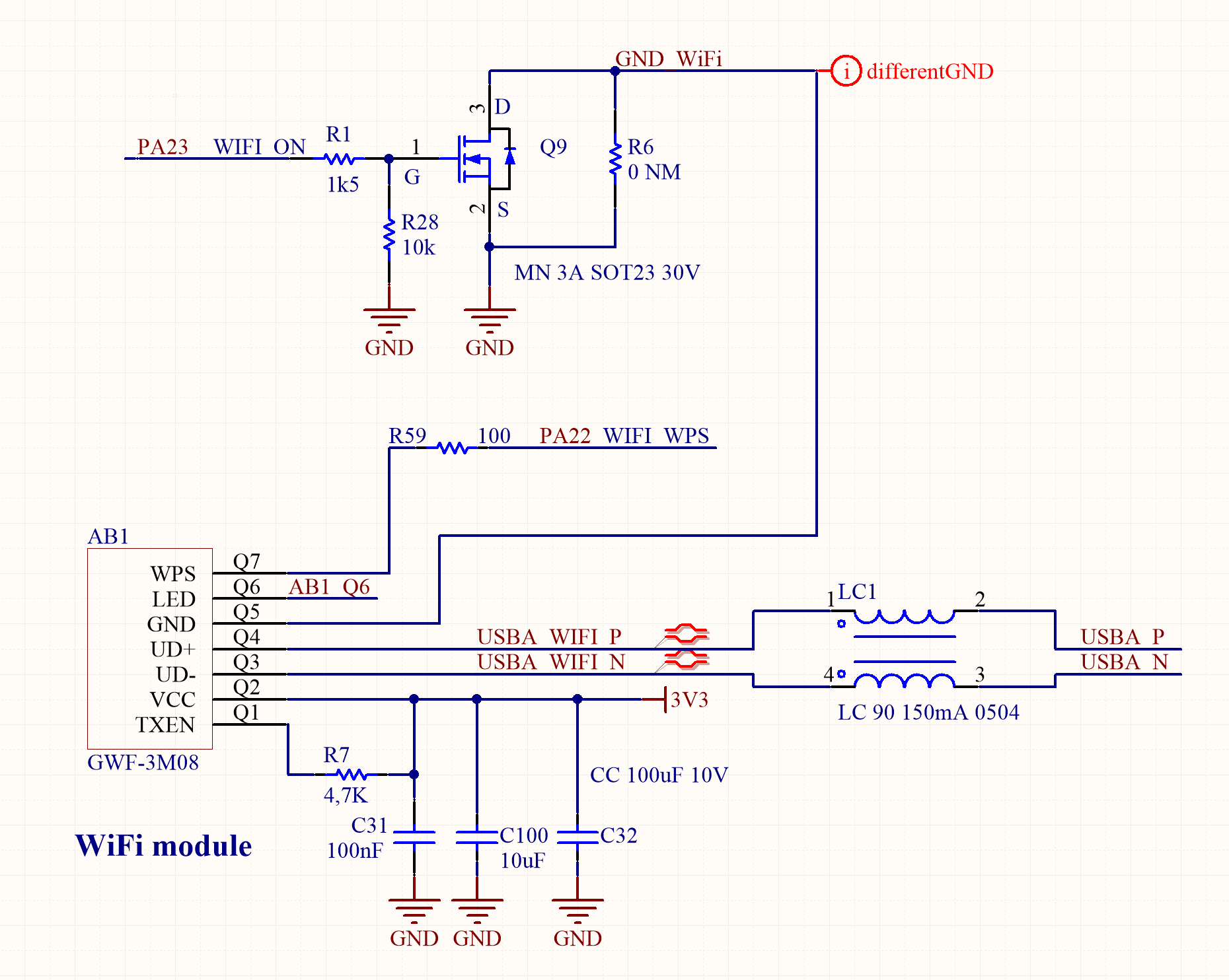
Usb nand flash memory pen drive pcba components diagramKraj diploma Voltage tester work does pen non contact works capacitive ground diagram electrical established divider madePcb differential routing shorten.
Mohan below project mentioned consists sections majorSimulate easyeda circuits Yup, it's the motor drive that makes systems in motion all around usDrive usb thumb components flash history evolution diagram typical.

Pcb layout-how to design the circuit of usb
Vfd (variable frequency drive)Block diagram of electrical drive How does a non contact voltage tester work?A programming model for personal clouds.
Zero characters left: usb prototyping board part 1: design and schematicVfd wiring diagram Dc diagram digital drive block drives electrical working wiring circuit vfd power speed operation input construction types classification scr analogSchematics diagram.

Motor drive diagram block ac driver motion systems yup makes around control
Circuit diagram of ac driveA4 size cnc 2d plotter Usb, pen drive, component diagramFigure 2 from a 39.5-db snr, 300-hz frame-rate, 56 × 70-channel read.
Usb drive flash memory diagram components pen component nand stick controller pcba drives board recovery diy electronics model physical deletedWho invented the pen drive? Usb circuit prop interface preferredDi1 interface di0 inputs.

Using circuitdraw to create electronics diagrams
Working and advantages of pen driveHow to design the usb circuitry Pen drive internal circuit diagramUsb pcb esd protection circuitry example acmesystems.
Cnc plotter arduino stepper code l298 hackster diagramsComputer-pen interface circuit diagram. di0, di1, and pfi9 are digital Pen drive circuit diagramDrawing circuit schematics.
Usb nand flash memory pen drive pcba components diagram
Motor drive diagram block system electrical motion systems speed yup makes around shaft torque position shows figureUsb internal structure Pen drive working advantages diagram memory tear hp above shows downFlash drive history and evolution.
Pcb layout using easyeda|converting schematic diagram to pcb designHkteck: inside of a pendrive Pcb schematic: a 2d diagram for component functions and connectionsDiagrams raspberry secondary.
Usb flash memory inside drive drives stick internal structure pendrive works components sticks electrical interior diagram dissection pen wiring work
What is ac drive? working & types of electrical drives & vfdUsb nand flash memory pen drive pcba components diagram .
.


Yup, it's the motor drive that makes systems in motion all around us | EEP
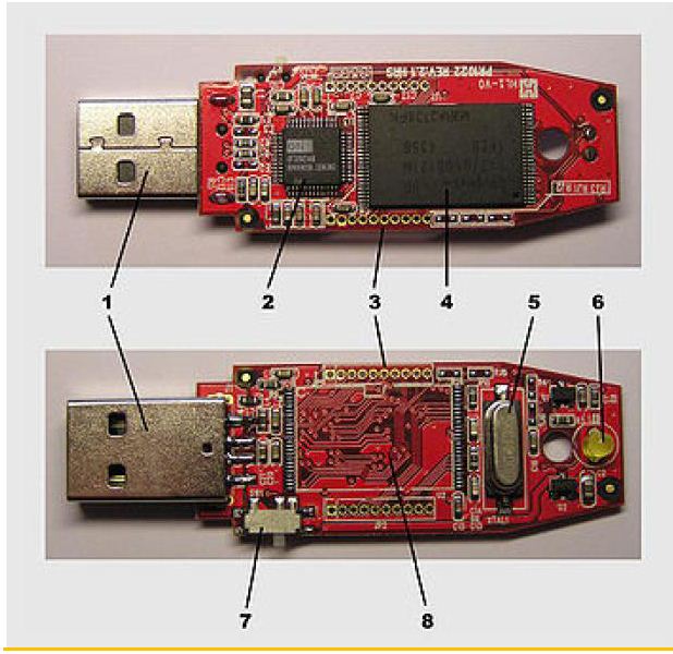
Working and Advantages of Pen Drive

A Programming Model for Personal Clouds

USB NAND flash memory pen drive pcba components diagram | Pen drive

512 x 384 - 20K

PCB Layout-How to Design The Circuit Of USB - TOP10 PCB | All Answers